42 register timing diagram
Timing diagrams and Machine cycles - Learn with 8085 ... The timing diagram of a typical OFMC is explained below. 1st T state During the first T state, the address of the location where the opcode is stored is loaded on the address bus. In 8085, this address is stored in a 16-bit register called the program counter. Basic Tutorial Lesson 10: Building a Shift Register Using ... The 4-bit shift register circuit. Your timing diagram will look like the figure below. As you can see from the figure, after the input is set high at t = 100ns for the first time, it takes the first flip-flop until the clock's next rising edge at t = 200ns to react. The first output B0 rises to 1 at t = 214ns (tPLH = 14ns).
Shift Register Timing Diagram - U Wiring The timing diagram shows the operation the Bi-directional shift register which initially shifts data towards the left. The part that runs to infinity and beyond void loop incoming read_shift_regs. Here each flip-flop stores an individual bit of the data in appearing as its input FF 1 stores B 1 appearing at D 1.

Register timing diagram
Serial to Parallel Converter - 4-bit Shift Register Serial to Parallel Converter - 4-bit Shift Register. A serial to parallel converter is a digital circuit where we feed the input data serially, and read the outputs in parallel fashion. A 4-bit serial-to-parallel shift register is one of the simplest types of circuits utilising four D-type flip-flops. Shift registers are widely in use in modern ... PDF DDR2 SDRAM Device Operating & Timing Diagram prior to writing into the mode register. The mode register set command cycle time (tMRD) is required to complete the write oper ation to the mode register. The mode register contents can be changed using the same command and clock cycle requirements during normal operation as long as all banks are in the precharge state. What is timing diagram 8085? - JanetPanic.com Timing Diagram is a graphical representation. It represents the execution time taken by each instruction in a graphical format. The execution time is represented in T-states. Instruction Cycle: The time required to execute an instruction . Machine Cycle: The time required to access the memory or input/output devices .
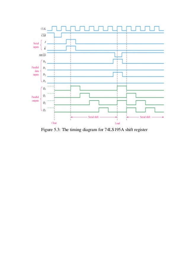
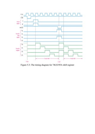
Register timing diagram. Solved The timing diagram below is for the 8-bit register ... Computer Science questions and answers. The timing diagram below is for the 8-bit register block shown. Complete the timing diagram by filling in the output (g) signal. 2. U1 load q (N-1:0) clr d (N-1:0) Signal name clk clr 4080120 160200240280' F5 18 DA load. Question: The timing diagram below is for the 8-bit register block shown. WaveDrom - Digital timing diagram everywhere WaveDrom draws your Timing Diagram or Waveform from simple textual description. It comes with description language, rendering engine and the editor. WaveDrom editor works in the browser or can be installed on your system. Rendering engine can be embeded into any webpage. PDF Shift registers - Griffith University Figure 5.3: The timing diagram for 74LS195A shift register . 6.0 Bidirectional Shift Registers The registers discussed so far involved only right shift operations. Each right shift operation has the effect of successively dividing the binary number by two. If the operation is reversed (left shift), this has the effect AN-CM-303 8-bit SISO, SIPO, PISO, PIPO Shift Registers ... The timing diagram of the PIPO shift register is shown in Fig. 8. As all the inputs and outputs are loaded and unloaded separately, it results in a large number of waveforms to show. The yellow highlighted line in the waveforms separates the input and the output. All the top waveforms are inputs and the bottom waveforms are outputs.
PDF Principles Of Digital Design - University of California ... Shift Register Timing . Register File Timing . RAM . Up/Down Counter . FIFO Queue . RTL Storage Components DIGITAL DESIGN 101, University of California Problem: Complete the timing diagram for the shift register shown. Assume the register stores 0's initially and inputs I L and I R are always 0. Shift Register Timing Present State . Operation ... COA | Register Transfer - javatpoint The following image shows the block diagram that depicts the transfer of data from R1 to R2. Here, the letter 'n' indicates the number of bits for the register. The 'n' outputs of the register R1 are connected to the 'n' inputs of register R2. A load input is activated by the control variable 'P' which is transferred to the register R2. Shift Registers in Digital Electronics - Javatpoint Shift Register. A group of flip flops which is used to store multiple bits of data and the data is moved from one flip flop to another is known as Shift Register.The bits stored in registers shifted when the clock pulse is applied within and inside or outside the registers. Help me understand this shift register timing diagram On every clock pulse, the state of the serial data pin is read As data is read, it gets shifted in to the registers When the latch pin pulses the values in the register are sent to the parallel output pins Here is a timing diagram for the 74HC595. SH_CP is the clock, and DS is the serial data pin.
PDF L7: Memory Basics and Timing - Massachusetts Institute of ... L7: 6.111 Spring 2004 Introductory Digital Systems Laboratory 5 Static RAM (SRAM) Cell (The 6-T Cell) WL BL VDD M5 M6 M4 M1 M2 M3 BL Q Q State held by cross-coupled inverters (M1-M4) Retains state as long as power supply turned on Feedback must be overdriven to write into the memory WL BL BL WL Q Q Write: set BL and BL to 0 and V Register to Register Path - timing diagrams Register to Register Timing Diagram with Clock Frequency at 20MHz The list below shows the delays and constraints that need to be considered for setup analysis of the path from register 1 to register 2. R1 Clock-to-Q Delay Maximum CL Propagation Delay Maximum R2 Setup Constraint Minimum Tc The Clock Period Minimum (1)¶ Timing Diagram - 8085 Microprocessor Course Read and write timing diagram for memory and I/O Operation Memory Read: >Figure: Memory read timing diagram Operation: It is used to fetch one byte from the memory. It requires 3 T-States. It can be used to fetch operand or data from the memory. During T1, A8-A15 contains higher byte of address. At the same time ALE is high. Universal Shift Register : Design, Working & Its Applications Universal Shift Register Diagram. Serial input for shift-right control enables the data transfer towards the right and all the serial input and output lines are connected to the shift-right mode. The input is given to the AND gate-1 of the flip-flop -1 as shown in the figure via serial input pin.
Shift registers
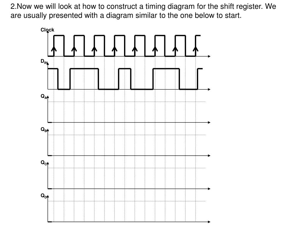
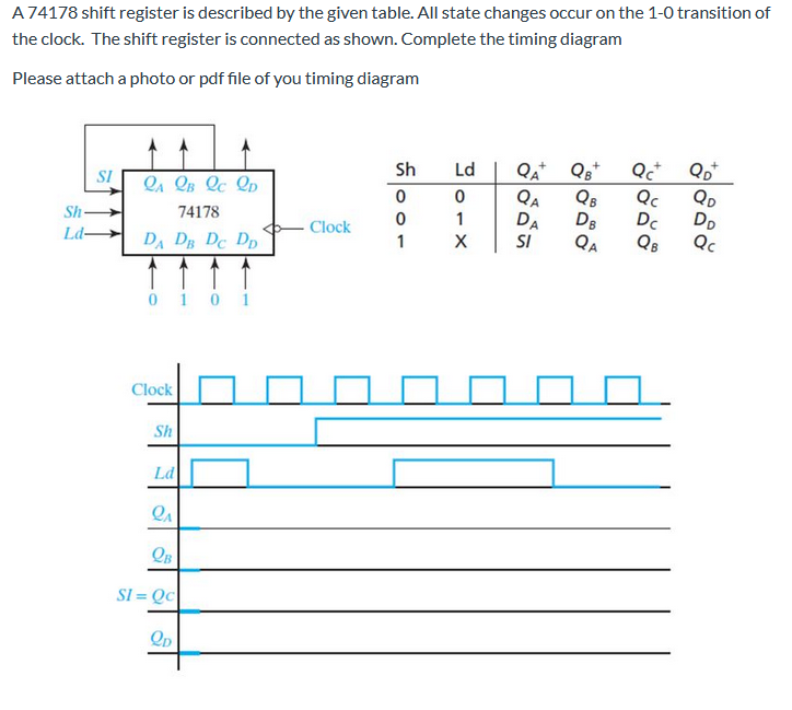
PDF Registers and Counters - Islamic University of Gaza timing diagram for a shift register. 3. Explain the operation of binary counters, show how to build them using flip-flops and gates, and analyze their operation. 4. Given the present state and desired next state of a flip-flop, determine the required flip-flop inputs.
ShareTechnote
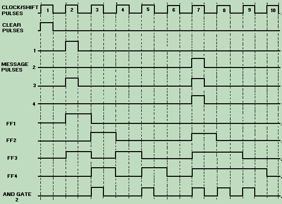
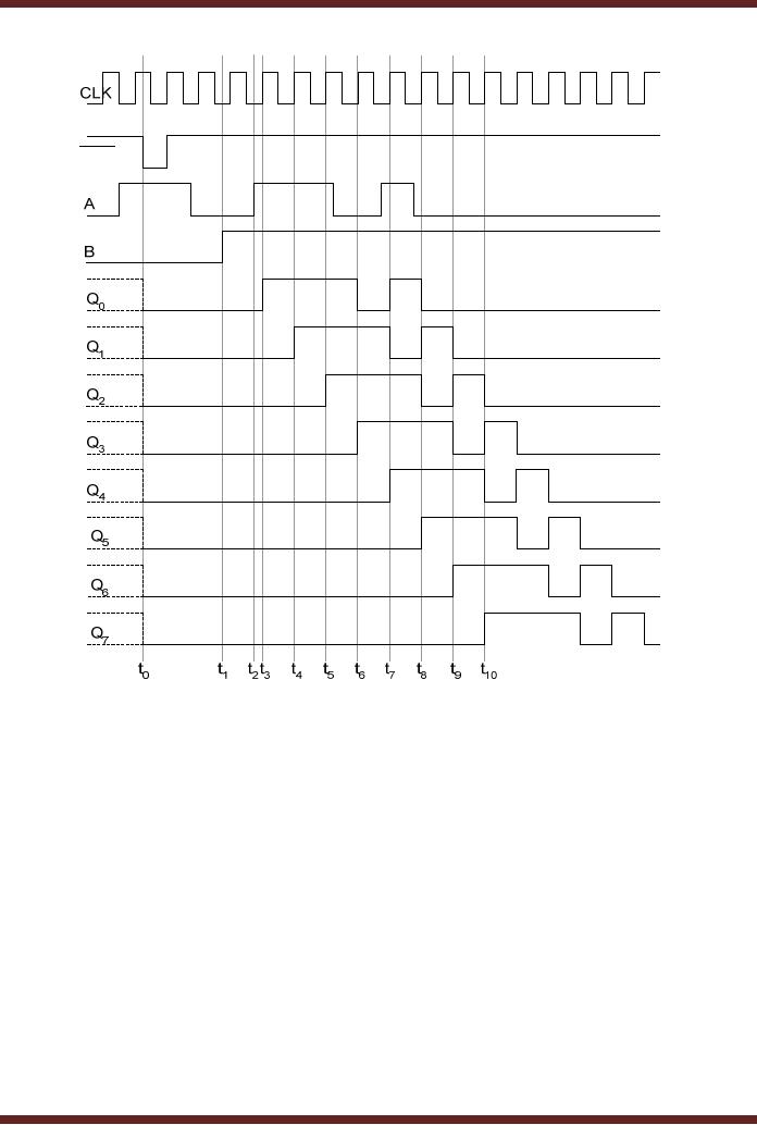
SHIFT REGISTERS:Serial In/Shift LeftRight/Serial Out ... In the timing diagram, the register is cleared asynchronously by activating the active-low CLR input at interval t 0. The serial data is applied at input A of the register before interval. t 0. However, the register is enabled to perform shift operation at interval t 1, when input B is set. to logic high.

Dynamic Shift Register | Electrical4U
How to Read Timing Diagrams: A Maker's Guide | Custom ... As you can see, the timing diagram is an addition to the textual description to make it easier to visualize the operation of the device. Knowing this, let's continue by looking at the counting process. In this example, the counter is preset to twelve: As you can see, the input data was present long before the load operation was triggered.

Shift Registers: Parallel-in, Serial-out (PISO) Conversion ...
Timing Diagram Explained | EdrawMax Online Source:EdrawMax Diagram 2: Boat manufacturing process. 4. Conclusion One of the key benefits of a UML timing diagram is that it gives users an overview of what goes on in a system or piece of software. More critically, it shows which steps in a system take too much time, and this information can be used by business users and developers alike to improve their processes.
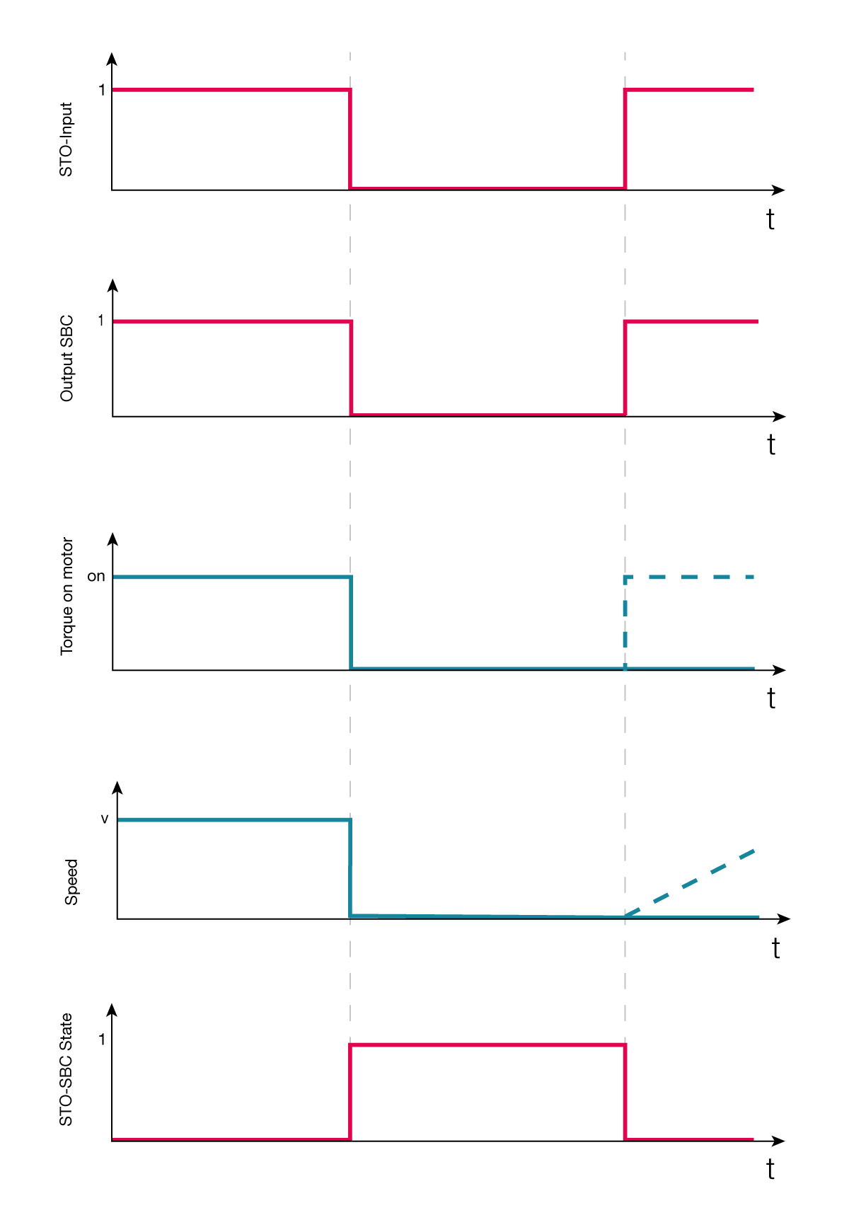
Using the safety functions — Synapticon Documentation
Register File Timing Diagram - YouTube Example trace of a timing diagram for a register file
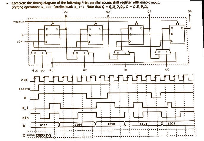
Solved) : Complete Timing Diagram Following 4 Bit Parallel ...
Timing Diagram Basics - Rheingold Heavy What is a Timing Diagram. Timing Diagrams are a way to symbolically represent the activity of one or more signals being transmitted or received by a component, and the way they relate to each other over a span of time. Any device that communicates with other devices over serial communications methods will include them in their datasheet.
![products:w7500:peripherals:pwm [Document Wiki]](http://wizwiki.net/wiki/lib/exe/fetch.php?media=products:w7500:peripherals:pwm_timing_diagram2.jpg)
products:w7500:peripherals:pwm [Document Wiki]
Timing Diagram - an overview | ScienceDirect Topics Janis Osis, Uldis Donins, in Topological UML Modeling, 2017. 1.2.2.7 Timing Diagram. Timing diagram is used to show interactions when a primary purpose of the diagram is to reason about time; it focuses on conditions changing within and among lifelines along a linear time axis. Timing diagram is a special form of a sequence diagram. The most notable graphical difference between timing diagram ...

Shift Register
What is Shift Register? Working, Applications & Types of ... The 74HC194 Bi-direction shift register is a good example. The register can operate in all the modes and variations of serial and parallel input or output. The functional diagram of the 74HC194 highlighting the control line, clock, input and output pins is shown below. The timing diagram of the device is also shown below.

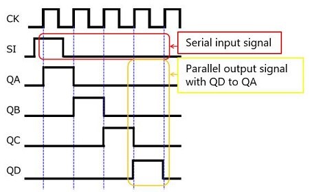
1 CHAPTER 12 REGISTERS AND COUNTERS This chapter in the book ...
PDF Device Operation & Timing Diagram - Samsung us MRS Mode Register Set Write A WRA,WRAS4, WRAS8 with/without CRC SRX Self-Refresh exit REF Refresh, Fine granular-ity Refresh RESET_n Start RESET procedure MPR Multi Purpose Register TEN Boundary Scan Mode Enable . MPSM. VrefDQ training TEN RESET ZQCL ZQCS,ZQCL Automatic Sequence Command Sequence. PDA. MPSM. IVREFDQ, RTT,Etc. mode. w/ DQ0=Low ...
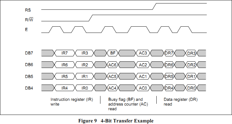
hd44780 timing diagram - PIC18 Tutorials - Gallery - FoxyTronics
Timing Diagram Software | Create UML Timing Diagrams ... Draw timing diagrams with minimal effort. Advanced features to simplify creating even the most complex of timing diagrams with amazing ease. Smart shapes and connectors, plus create and multiple diagramming shortcuts. Drag and drop interface with a contextual toolbar for effortless drawing. Intuitive swimlane shapes and grids with precision ...
CHAPTER 1
Shift Registers Worksheet - Digital Circuits This question reviews the principles of D-type flip-flops, timing diagrams, and serves as an introduction to shift registers. Question 5 What is the definition of a register in the context of digital circuitry?

MICSY S-logic
What is timing diagram 8085? - JanetPanic.com Timing Diagram is a graphical representation. It represents the execution time taken by each instruction in a graphical format. The execution time is represented in T-states. Instruction Cycle: The time required to execute an instruction . Machine Cycle: The time required to access the memory or input/output devices .
Write truth table, timing diagram and logic diagram of SISO ...
PDF DDR2 SDRAM Device Operating & Timing Diagram prior to writing into the mode register. The mode register set command cycle time (tMRD) is required to complete the write oper ation to the mode register. The mode register contents can be changed using the same command and clock cycle requirements during normal operation as long as all banks are in the precharge state.

Learn.Digilentinc | Shift Registers
Serial to Parallel Converter - 4-bit Shift Register Serial to Parallel Converter - 4-bit Shift Register. A serial to parallel converter is a digital circuit where we feed the input data serially, and read the outputs in parallel fashion. A 4-bit serial-to-parallel shift register is one of the simplest types of circuits utilising four D-type flip-flops. Shift registers are widely in use in modern ...
Shift registers
PPT - 4-4-3 Shift registers PowerPoint Presentation, free ...

datasheet - Help me understand this shift register timing ...
CHAPTER 1
Shift register
Solved) : 5 Timing Diagram Shift Register Consider Following ...

74HC595 8 bit Shift Register – Zx Lee

74LS166 8-bit Shift Register Pinout, datasheet, examples and ...
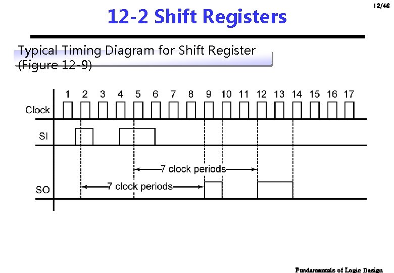
146 CHAPTER 12 REGISTERS AND COUNTERS This chapter

Smiley's Workshop 28: Gettin' A Little Shifty | Nuts & Volts ...
Sequential Logic: Shift Registers | Toshiba Electronic ...

Answered: 1) Draw timing diagram. Q0,Q1,Q2,Q3… | bartleby
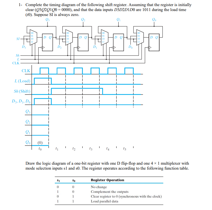
Solved 1. Complete the timing diagram of the following shift ...

What is Shift Register? Working, Applications & Types of ...

Shift Register - Parallel and Serial Shift Register
Registers

Shift register - Wikipedia
Shift register

Body
Solved: Need help with this question , if anyone can compl

5 Leon Register File Timing | Download Scientific Diagram
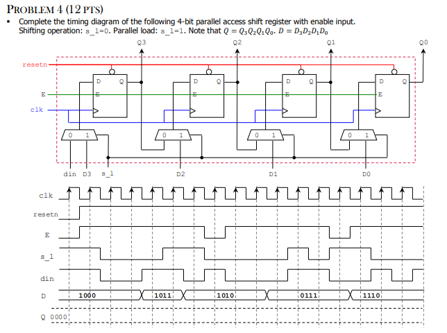
Solved) : Problem 4 12 Pts Complete Timing Diagram Following ...
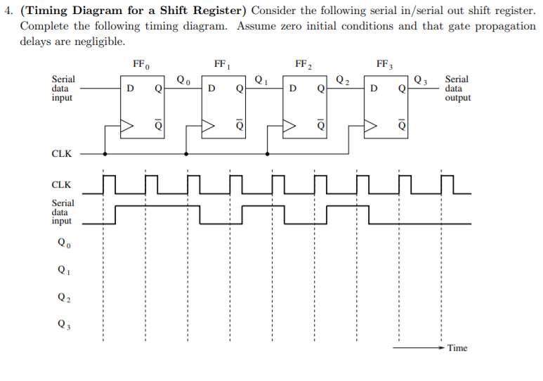
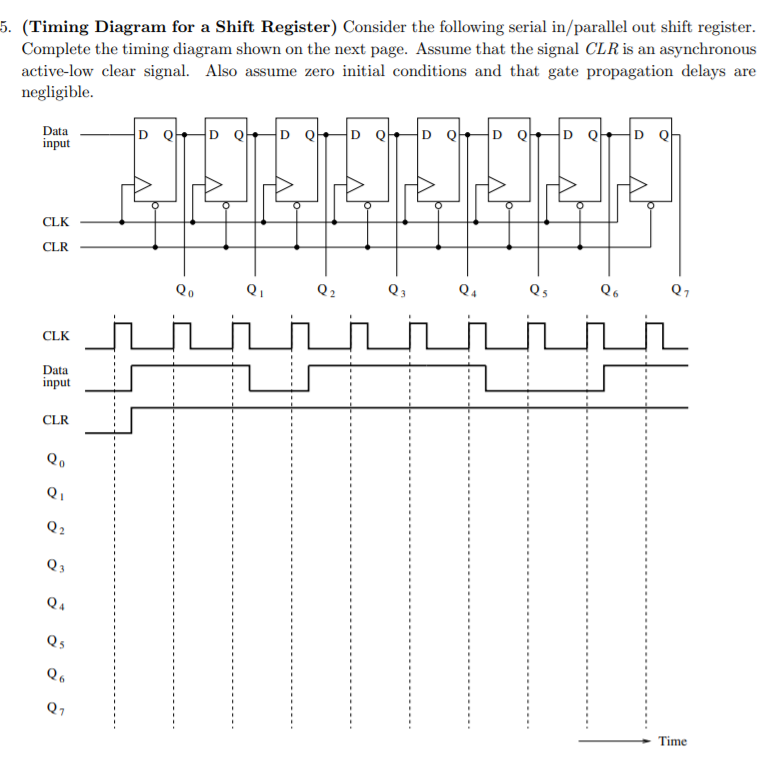
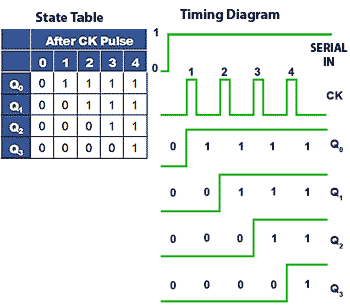
Solved 4. (Timing Diagram for a Shift Register) Consider the ...

Glossary of Electronic and Engineering Terms, IC Shift ...
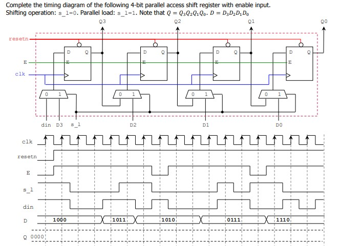
Solved) : Complete Timing Diagram Following 4 Bit Parallel ...

Using 74hc595 Shift Register with Raspberry PI
SHIFT REGISTERS:Serial In/Shift LeftRight/Serial Out ...
Shift registers


Comments
Post a Comment