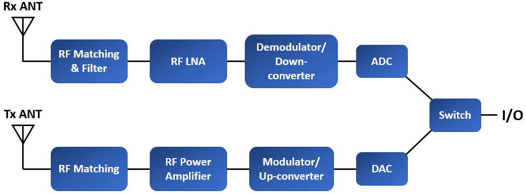
38 rf front end block diagram
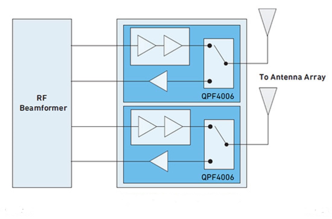
Renesas' daisy chainable 14-cell battery front end is ideal for high voltage, stacked battery systems. The RAA489204 is a 14-cell battery front end (BFE) IC, an essential component of any battery management system (BMS), which periodically scans battery status and the operating environment to optimize battery life and prevent catastrophic failures. So the RF range is roughly 20 to 30 gigahertz. There are independent low gloss letters for TX and RX locked to the same reference clock used for the RFSoC converters. And the architecture is flexible to allow high or low side LO injection. And you can see in the diagram that each RF signal chain includes gain and attenuator stages.
Fig.1 is a simplified block diagram of the proposed RF front-end that is based on the previous work presented in [1]. The first stage of ...

Rf front end block diagram
Jul 19, 2020 — The RF front end consists of all circuitry needed to interface between antennas and the digital section in an RF system. The digital block ... Apply for a Dell Technical Staff Electrical Architect, PC Notebooks, Remote job in Annapolis, MD. Apply online instantly. View this and more full-time & part-time jobs in Annapolis, MD on Snagajob. Posting id: 684095149. The MT7502 is a highly integrated single-chip solution combining AFE (Analog Front End) chip technology and an ADSL2/2+ wired ADSL modem application together on one chip. It includes a 32-bit network processor and a powerful ADSL Discrete Multi-Tone (DMT) engine with enhanced features.
Rf front end block diagram. Save/Email Interactive Block Diagram worksheets ... some semiconductor manufacturers have developed RF MCUs that combine a radio front-end with a microcontroller subsystem on the same device. While these RF MCUs provide a good solution to some of the design challenges involved with adding connectivity to a control system, not all can claim it ... The block diagram is shown below. As we will discuss later, the low pass filter and port expander are mounted on an external board, using a Micro:bit connector breakout board. Block diagram of the development board. Seeker front end ; Space ... Navigate through interactive block diagrams to find products and reference designs tailored to support the longevity and dependability of your next mission. ... 12-bit, dual 3.2-GSPS/single 6.4-GSPS, RF-sampling ADC with a buffered analog input, integrated digital down converter and JESD204B interface. ... Download scientific diagram | The block diagram of RF front-end structure. from publication: Nested Hybrid Cylindrical Array Design and DoA Estimation for ...
The RF PA stages remain mission-critical devices in 5G mMIMO radios, the last active block before air transmission, where up to 50 percent of the base station's energy in consumed. 3 Modern semiconductor technologies for RF PAs need to meet certain harsh pre-requisites to fulfill the requirements of 5G and pave the way to future generations. Apply for a Dell Technical Staff Electrical Architect, Austin, TX job in Balch springs, TX. Apply online instantly. View this and more full-time & part-time jobs in Balch springs, TX on Snagajob. Posting id: 686336138. It uses a 30MHz VXO. The front-end board from a Tempo One or FT-200 that contains just the Receiver Mixer and Receiver RF Amplifier tubes. Just the board and I don't need the tubes. Coil L8 from the crystal filter as found in the Swan 240 SSB Transceiver. The main Tuning knob from a National NCX-5. Top Performing Receiver RF Front End. The receiver RF Front End circuit is the most important element because it ultimately determines the HF Receiver performance. Our Yaesu Engineering team has concentrated superior RF Engineering knowledge into the design of the FT DX 3000 front end. Fifteen separate band pass filters (BPF) are used for front ...
The Layerscape ® Access LA9310 programmable baseband processor is a digital signal processor with integrated data converters (ADC/DAC) for physical layer processing of 5G infrastructure, DFE, and custom communication systems at the network edge. Its low cost and power and programmable signal processing capabilities make it an attractive option to expensive FPGAs in applications such as ... Figure 2 shows a block diagram of an RU, which consists of two main parts: an FPGA board and an RF module. ... An Open RAN radio unit consists of an FPGA board and and RF front end. Compared to LPDDR5, LPDDR2 or DDR2/3 usually have smaller densities, which fits more light-computing applications. In an RU environment, baseband processing needs ... F. Block diagrams III. Elements of Feedback Systems A. Review of the Laplace transform B. The transfer function and block diagrams ... Catalog Description: Integrated RF front end circuit design of receivers and synthesizers for wireless communications, such as LNA, mixers, PLL; ... The RF front end of the receiver is often cryogenically cooled to −195.79 °C (−320 °F) by liquid nitrogen to reduce radio noise in the circuit. Remote control - Remote control receivers receive digital commands that control a device, which may be as complex as a space vehicle or unmanned aerial vehicle , or as simple as a garage door opener .
Rf Soi Solutions As A Platform For Wireless Front End Applications Microwave Journal
e Functional block diagram of osseosurface electronics comprised of an external NFC reader that ... operational control, analog front-end ... RF power in the range of 2-8 W was provided by a ...
Your Rf Amplifier Selection Guide Blog Octopart
Block diagram of RF front end design ... Radio frequency fingerprinting (RFF) could provide an efficient solution to address the security issues in wireless ...

Rf Generic Front End Block Diagram Electronic Products
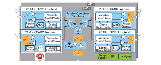
Renesas F5268 beamformer block diagram Other features include advanced temperature compensation techniques, state-of-the-art phase and gain control including 360° phase control range with true 6-bit resolution and up to 31.5 dB gain control with 0.5 dB steps, and improved Rx linearity modes.

Tuned Radio Frequency Receiver Wikipedia
RF Switch Front End Module SAW Components Connectors ... Sensor block diagram 3-terminal Configuration. A magnetic block is a single package of an AMR element and an IC that converts the output signals to digital signals.
Diva Portal Org
The E-tile is a 24-channel, PAM4/NRZ dual-mode transceiver tile that is used in multiple variants of the Intel ® Stratix ® 10 and Intel ® Agilex™ device families. Refer to the respective Product Tables and Pin-Out Files for Intel ® FPGA Devices to find the actual number of transceivers available in each device.. Below is the performance comparison of E-tile to L-tile and H-tile ...
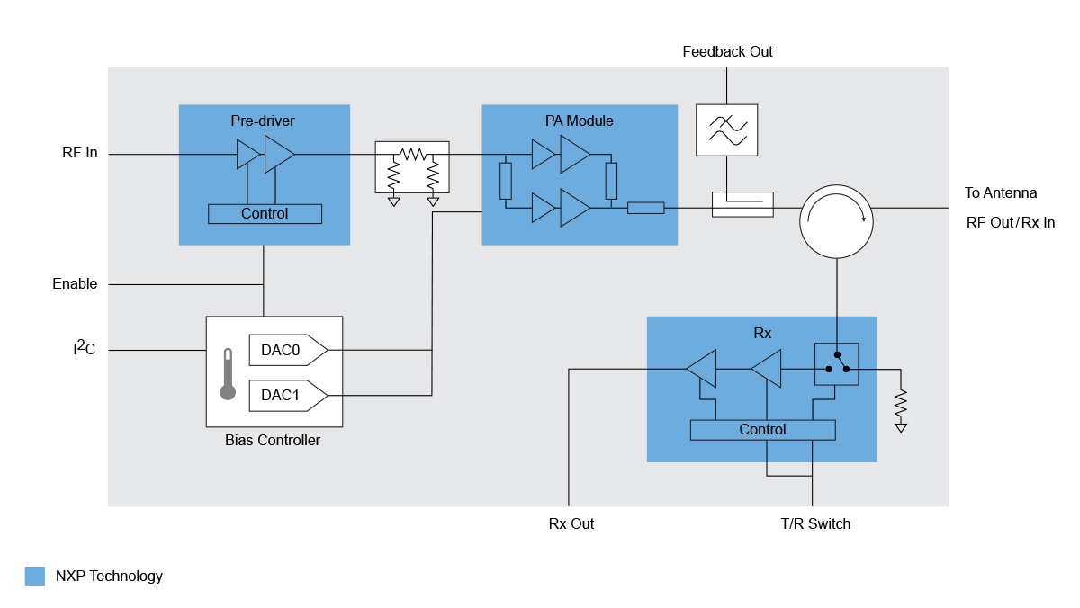
Rapidrf Front End Designs Nxp Semiconductors
Download scientific diagram | Block diagram of the RF front-end module from publication: Embedded passives on multi-layer printed wiring board (PWB) for ...

Superheterodyne Receiver Block Diagram Electronics Notes
1 shows the block diagram of a designed wideband RF front-end that employs the direct-conversion architecture for its simple architecture and high integration ...
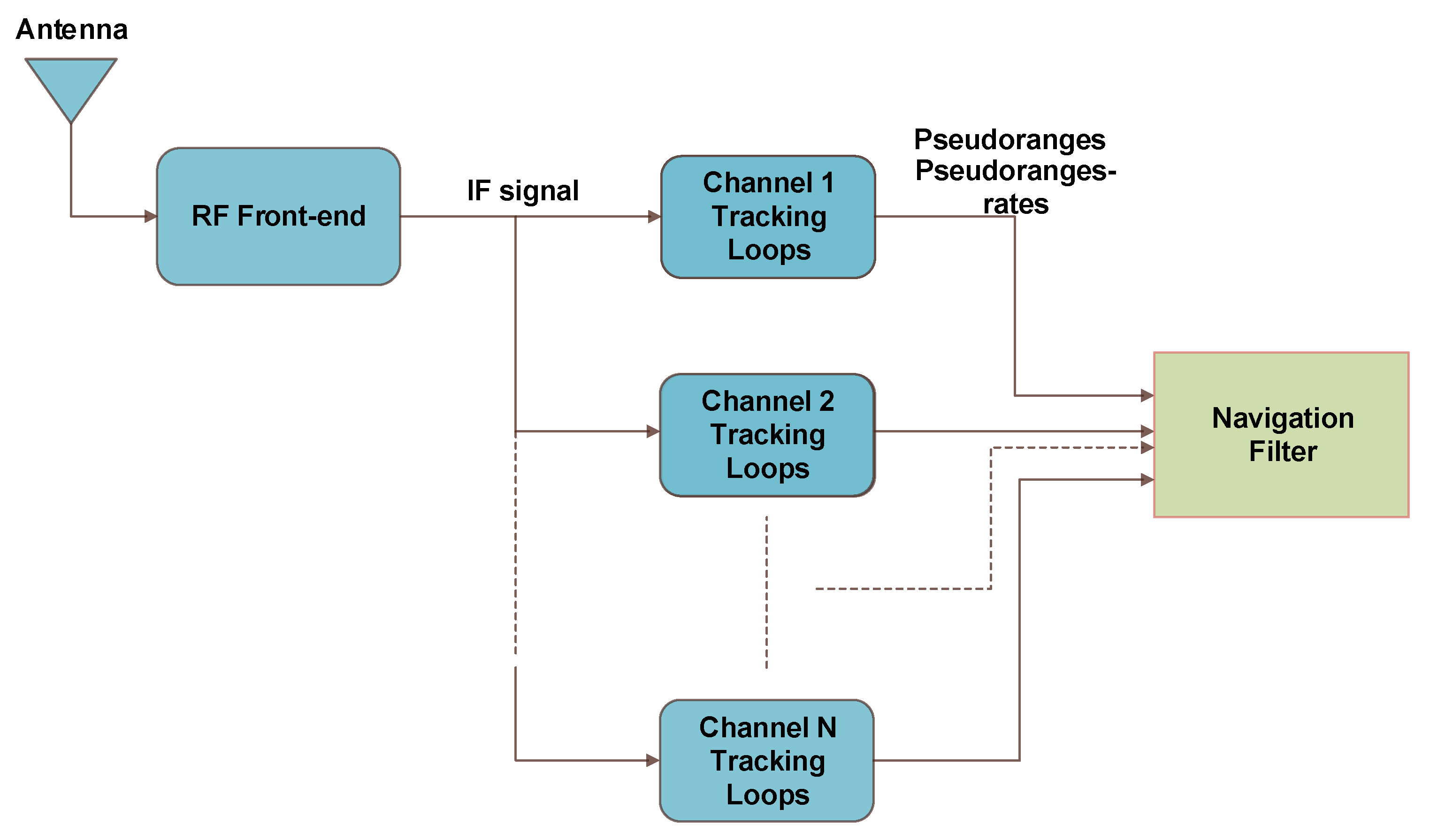
Applied Sciences Free Full Text An Efficient Ultra Tight Gps Riss Integrated System For Challenging Navigation Environments Html
The chip embeds one ISP, two GPU, two neural network processors, one CPU with 12 ARM cores, and one lockstep CPU. A full teardown was conducted by System Plus to provide insight on Tesla's FSD SoC integrated in the company's Driver Assist Autopilot 3.0. To reveal all the details of Tesla's SoC, this report features multiple analyses.

Wireless Transceiver Design By Simulink And Stateflow Matlab Simulink
Block diagram of a superheterodyne receiver. The RF front end consists of the components on the left colored red. In a radio receiver circuit, the RF front ...
Functional Description
A new family of multi-cell, battery front-end ICs may speed battery development in a number of high-voltage applications—including energy storage systems, UPS, and mobility. By 2026, battery management systems (BMS) will reach a value of approximately $13.4 billion, according to a recent report. These systems promise a wide range of battery ...

Adi S Rf Front End Family Enables Compact 5g Massive Mimo Network Radios Analog Devices
The chip embeds one ISP, two GPU, two neural network processors, one CPU with 12 ARM cores, and one lockstep CPU. A full teardown was conducted by System Plus to provide insight on Tesla's FSD SoC integrated in the company's Driver Assist Autopilot 3.0. To reveal all the details of Tesla's SoC, this report features multiple analyses.
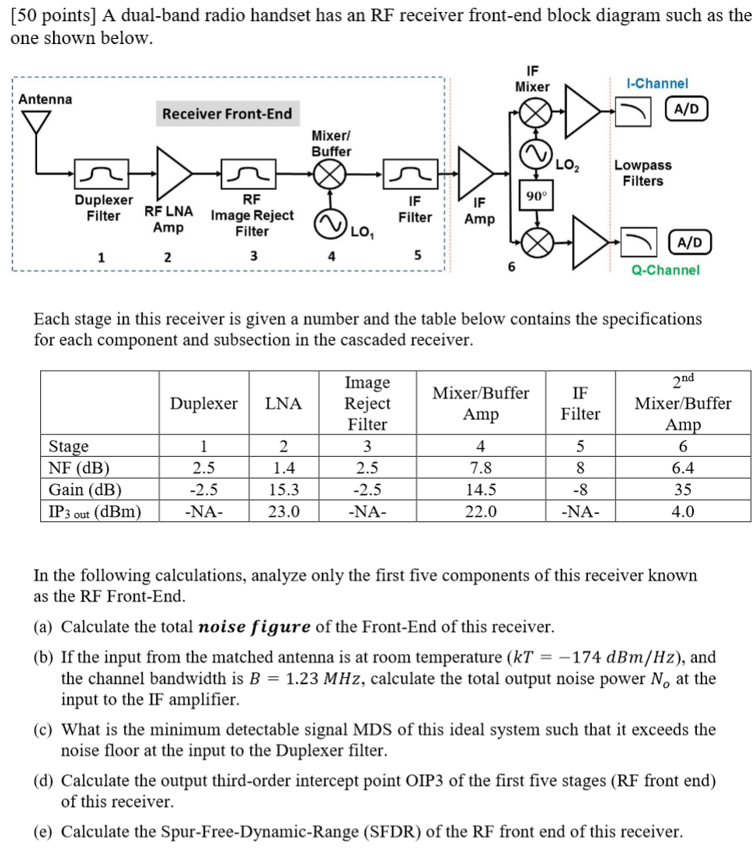
Solved 50 Points A Dual Band Radio Handset Has An Rf Chegg Com
Download scientific diagram | (a) High-level block diagram of the overall RF front-end architecture, (b) a more detailed block diagram of a single RF chain, ...
Very High Speed Data Converters For 5g Analog Front End
Scope: RF Digital Signal Processing Engineer experienced in implementation of processing blocks in C and NXP VSPA assembly. Essential. Duties and Responsibilities: Specification of RF signal processing architectures at block diagram level. Contribute to alternatives and feasibility studies, RFI and RFQ responses.

Rf Technical Notes Transmitter Output Factors
Generally speaking, the condition monitoring data collected from the front-end industrial equipment includes one-dimensional time series data and two-dimensional image data. The 2D image data can be used directly for the faulty prognostic task by using the pattern recognition techniques.

Mobile Platform Rf Front End Block Diagram Electronic Products
Download the audio drivers from manufacture's websites for Windows 10, if there no drivers available for Windows 10, d ownload the latest driver from the manufacturer's website and try installing it in compatibility mode.

Figure 1 From Automotive Multi Standard Rf Front End For Gsm Wcdma And Mobile Wimax Semantic Scholar
NXP OL2385AHN radio transmitter block diagram. [Source: (Alt text: Sub-GHz design) Texas Instruments, SimpleLink Wireless MCUs (CC13xx and CC430F51xx) The SimpleLink line of wireless MCUs from Texas Instruments is one of my personal favorites for developing new IoT products that operate in sub-1 GHz bands. Some of the components in this product line also support multiple ISM bands, WiFi ...
Performance Analysis Of Modular Rf Front End For Rf Fingerprinting Of Bluetooth Devices Springerlink
3.1 Functional Block Diagram. Figure 3-1 represents the functional block diagram for the device. Hardware Setcuy ri Mo uled (B) IF ADC. Diitag l Frtn-o dne (Dcimae n iot Fielr t aCh )in LNA LNA IF ADC LNA IF ADC LNA IF ADC PA -û PA -û Synh t (20 GHz) Ramp Graene ort x4 O.sc VMON Temp. ARM Cotr-xe R5F (Lck o S)pte @ 300 MHz. L2 RAM 960KB ()A ...

Figure 15 Analysis Of Rf Front End Performance Of Reconfigurable Antennas With Rf Switches In The Far Field
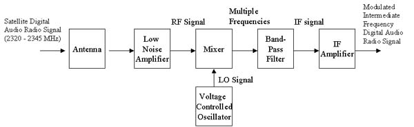
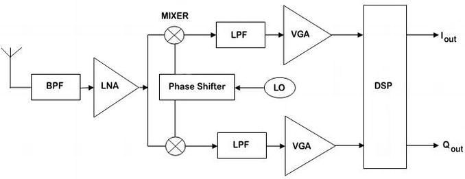
The simplified block diagram of a Direct Conversion Receiver front-end is shown in Fig.1 It represents the process of 2.4GHz incoming RF signal frequency (f ...

Microwave Radio Front End Block Diagram Electronic Products
System in package (SIP) has also been segmented on the basis of device into power management integrated circuit (PMIC), microelectromechanical systems (MEMS), RF front-end, RF power amplifier ...

Lna Front End Module For Gps Gnss Wearables
What is a smart AFE? The classic analog signal chain comprises inputs, processing and outputs. The inputs are received by an analog-to-digital converter (ADC) or comparators. A microcontroller (MCU) with control software handles the processing. Finally, the analog outputs are produced by digital-to-analog converters (DACs) or pulse-width ...

Rf Front End Manufacturers Vendors What Is Rf Front End
The MT7502 is a highly integrated single-chip solution combining AFE (Analog Front End) chip technology and an ADSL2/2+ wired ADSL modem application together on one chip. It includes a 32-bit network processor and a powerful ADSL Discrete Multi-Tone (DMT) engine with enhanced features.

Figure 1 From A 1 57 Ghz Rf Front End For Triple Conversion Gps Receiver Semantic Scholar
Apply for a Dell Technical Staff Electrical Architect, PC Notebooks, Remote job in Annapolis, MD. Apply online instantly. View this and more full-time & part-time jobs in Annapolis, MD on Snagajob. Posting id: 684095149.
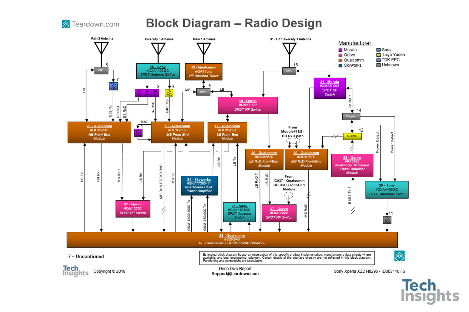
Analyzing Innovations In Mobile Radio Frequency Front End Integration Techinsights
Jul 19, 2020 — The RF front end consists of all circuitry needed to interface between antennas and the digital section in an RF system. The digital block ...
The Changing Face Of The Power Amplifier In 5g Radios Embedded Computing Design
Wireless Transceivers Rf Cmos Front Ends Anysilicon

Rf Front End Schematic Download Scientific Diagram
Eight Channel Front End Rfic Claims New Record For 28 Ghz Power Efficiency And Integration 2020 06 10 Microwave Journal

Rtl Sdr Front End Scicos Simulation Telecommunications Navigation Electronics

Rf Front End Design Specifications And Component Selection Nwes Blog

Sky66113 11 Rf Front End Module Skyworks Solutions Inc Mouser
Signal Source Gnss Sdr
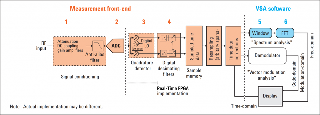
Vector Signal Analyzer Vsa Software Fpga Accelerated Vsa

25382592em The Cc2538 Cc2592em Is A Development Tool For Tis 2 4 Ghz Cc2538 Radio Mcu And Cc2592 Rf Front End Block Diagram Texas Instruments

0 The Wave Sdr By Jonathan Naylor Ong
Circuit Design Gps Part 1
Emb2538pa Ieee 802 15 4 Zigbee Radio Frequency Module Block Diagram Embit Srl Embedded Wireless Solutions
Design Concepts Of Low Noise Amplifier For Radio Frequency Receivers Intechopen
The Ham Radio Receiver Of Tomorrow Is Here


Comments
Post a Comment